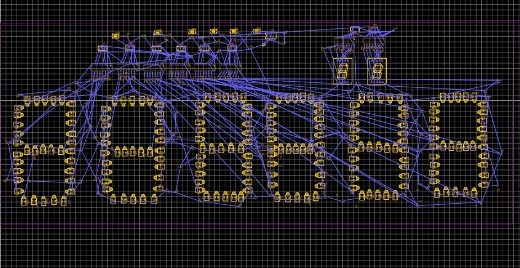
This image shows the pcb design the team made with EasyEDA. It shows the traces of the connections made and the components used.
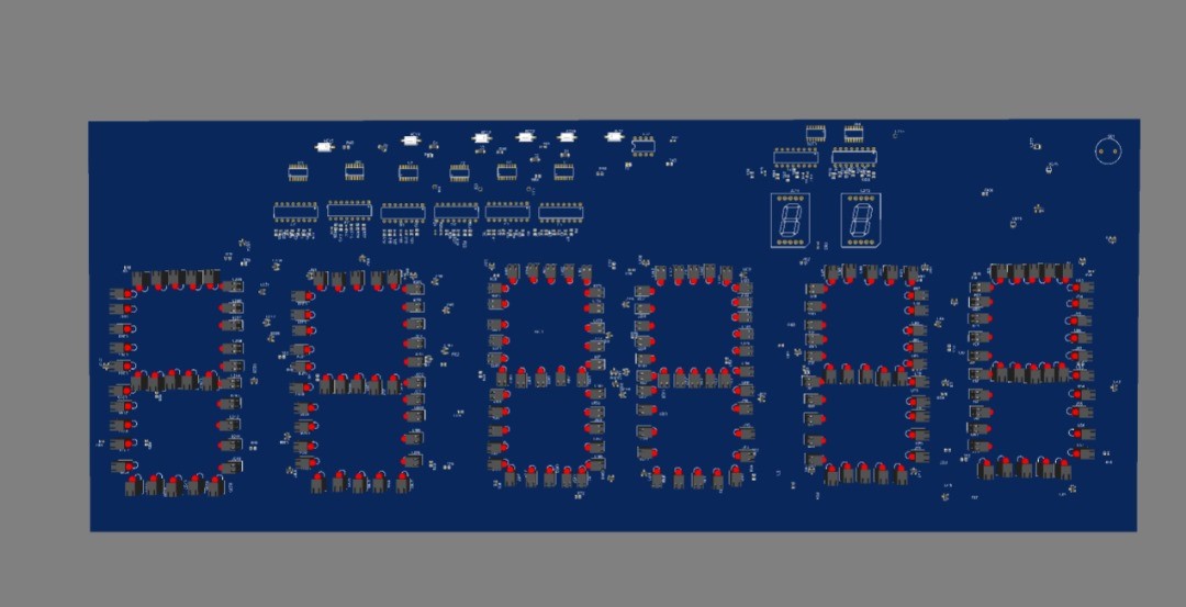
This is image shows the pcb design once more in EasyEDA but in the 3D model form which shows how the board, if implemented, would potentially look like.